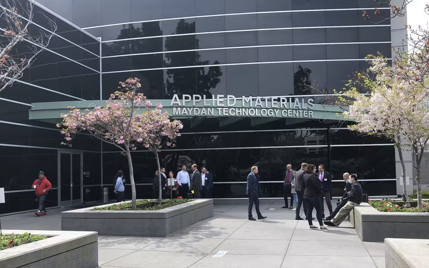
Applied Materials and Besi said on 1 October that they had expanded their partnership, bringing Besi into Applied’s EPIC Center, where capital spending is expected to scale to approximately $5 billion as customer projects commence. The move extends a collaboration begun in 2020, according to Applied Materials’ announcement.
Key points
- Besi is joining the EPIC Center as an Innovation Partner, Applied Materials said.
- The companies plan to extend their work beyond die-to-wafer hybrid bonding to other bonding methods, chip integration and photonics interconnects.
- Applied expects capital spending on EPIC to scale over time to approximately $5 billion as customer projects commence.
Singapore partnership produced the Kinex system
The companies established a joint Hybrid Bonding Center of Excellence at Applied’s Advanced Packaging Development Center in Singapore in 2020. Applied says the work combined its semiconductor process expertise with Besi’s die placement, interconnect and assembly technology. The arrangement gave the two equipment makers an existing development programme to extend when they agreed to work together at EPIC.
Applied says the Singapore collaboration produced Kinex, an integrated system for bonding individual dies to wafers. Its contribution to that programme covered etch, planarisation, deposition and wafer cleaning, as well as metrology, inspection and particle defect control. Besi supplied technology for placing dies and assembling the resulting structures, according to Applied.
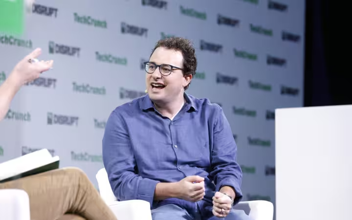
Gary Dickerson, Applied’s president and chief executive, said the EPIC arrangement would give both companies an earlier view of the technology roadmap’s direction. He said the companies intended to develop packaging processes together across more of the production flow. Richard Blickman, Besi’s chief executive and chairman of its board of management, described the Singapore centre as an important part of Besi’s hybrid bonding plans.
Besi engineers move into EPIC development work
As an Innovation Partner, Besi will have engineers working alongside Applied’s teams at the Silicon Valley centre, the companies said. They plan to broaden their work beyond die-to-wafer hybrid bonding to thermo-compression bonding and the processes around it. Applied also expects research programmes on new hybrid bonding platforms, using the companies’ Singapore work as a starting point.
The proposed integration platforms cover die-on-wafer, die-on-die and die-on-panel assembly. The companies also identified interconnects using photonics, including applications for co-packaged optics. Applied said the wider programme would focus on integrating logic and memory for AI computing systems, alongside the development of three-dimensional chip architectures.
Applied says the collaboration is intended to give customers earlier access to jointly developed process and assembly solutions. Those plans span wafer-level bonding through panel-scale integration. Prabu Raja, president of Applied’s Semiconductor Products Group, said putting Besi engineers in a front-end research facility would allow the companies to develop those stages as a connected production flow.
Blickman said joining EPIC would put Besi alongside logic, memory and systems companies as it worked on thermo-compression bonding, panel integration and interconnects. Applied describes higher-density, higher-bandwidth connections between chips and packages as a driver of the expanded programme for AI infrastructure.
Applied ties EPIC spending to customer projects
Applied describes the EPIC Center as a research and development facility for semiconductor equipment and process technology. It expects its capital spending on the centre to rise over time to approximately $5 billion as customer projects commence. The spending plan belongs to Applied, while Besi’s announced role is to contribute engineers to the joint development work.
Applied says the centre is designed to shorten the path from early research to manufacturing. The partnership’s planned work puts bonding equipment and the materials processes used around it in the same facility. Applied and Besi expect to develop solutions across that packaging flow for their mutual customers.
Applied identifies semiconductor demand, customers’ technology requirements and its ability to meet the centre’s objectives among risks to its plans. It also identifies the development and protection of new technology as factors that could cause results to differ from its expectations. Besi lists orders, shipments, expenses and the timing of customers’ equipment purchases among the subjects of its forward-looking statements.
Applied Materials expects the EPIC Center to be operationally ready in 2026.