South Korea broke ground on 12 November on the first project under its industrial megaproject programme, a 6 trillion won Samsung Electronics chip-packaging plant at Onyang, four months after the programme was unveiled, The Korea Herald reported. President Lee Jae Myung and Samsung Chairman Lee Jae-yong attended the ceremony at the company’s campus in Asan, South Chungcheong Province. The new line is intended to expand the site’s work beyond conventional chip assembly and testing into advanced high-bandwidth memory, or HBM, packaging.
Key points
- Samsung Electronics plans 46 trillion won of spending at Onyang, including 6 trillion won for construction and 40 trillion won for equipment.
- The fifth production line is targeted to start operating in June 2028, a year ahead of its original schedule.
- Samsung’s planned Chungcheong investment has risen to 144 trillion won from 140 trillion won announced in July.
- Samsung says customers are seeking more HBM for 2027 than the volumes already negotiated.
Onyang Line 5 targets June 2028
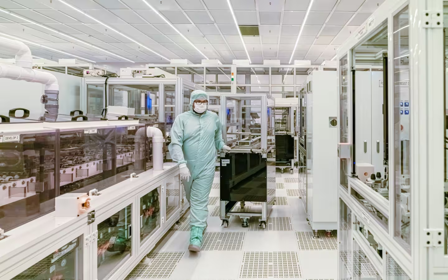
Samsung Electronics plans to invest 46 trillion won at Onyang: 6 trillion won to build the facility and 40 trillion won for advanced equipment installed in stages, The Korea Times reported. The fifth line is scheduled to begin operating in June 2028, one year earlier than originally planned. It will have about 31,000 square metres of cleanroom space across three floors.
The new line is planned to produce HBM4E chips, according to The Korea Herald. Lee Jae-yong said at the ceremony that the Onyang campus would move from its longstanding focus on assembling and testing conventional semiconductors towards advanced HBM production. Once the line is complete, the campus’s total floor area is expected to reach approximately 420,000 square metres, up from 270,000 square metres.
The facility is expected to create around 700 jobs. Building the facility is projected to bring 2.6 trillion won in economic output and provide work for an average of 3,400 people each day of construction, according to The Korea Times. Those projections concern construction activity and employment, separate from the equipment spending planned for the production line.
The government introduced three megaprojects in late June, covering semiconductors, AI data centres and physical AI, with the aim of directing investment beyond the Seoul metropolitan area. Lee said South Chungcheong Province and Asan had reduced permitting times to about one-third of their usual duration. At the ceremony, he pledged government work on permits and on electricity and water infrastructure for planned investments.
Samsung raises Chungcheong plan to 144 trillion won
The groundbreaking accompanied an increase in Samsung’s planned investment across the Chungcheong region to 144 trillion won, from 140 trillion won announced in July, Seoul Economic Daily reported. Samsung Electronics accounts for 60 trillion won of the revised plan across Onyang and Cheonan, up from its earlier commitment of 56 trillion won. The 46 trillion won planned for Onyang forms part of that wider electronics allocation.
The two publications give different dollar equivalents for the group’s 144 trillion won plan. The Korea Times puts it at $108 billion, while Seoul Economic Daily puts it at $98 billion.
In July, Samsung Electronics, SK Hynix and other major companies announced plans to invest roughly 392 trillion won in the central Chungcheong region. Lee has also sought backing for 21 trillion won in AI and megaproject spending, as AI Affairs previously reported.
HBM demand and the other Samsung plants
Samsung Electronics said during its third-quarter earnings announcement that negotiations over its 2027 HBM supply volumes were complete, but customers were requesting additional supplies. The company expects shortages to persist through 2028. The June 2028 target brings Onyang’s planned start into the period covered by that supply forecast.
Three other Samsung affiliates account for the rest of the revised regional plan. Samsung Display plans 67 trillion won for Asan and Cheonan, Samsung Electro-Mechanics 8 trillion won in Sejong and Samsung SDI 9 trillion won in Cheonan, according to Seoul Economic Daily. Their projects cover display panels, AI chip-package substrates and battery technology alongside Samsung Electronics’ memory and packaging investment.
Samsung Electro-Mechanics’ plan includes a new substrate factory accounting for 4.3 trillion won of its regional spending. Construction began in October, and the company is targeting mass production in September 2028. Samsung SDI’s Cheonan site is intended to develop next-generation battery technologies and test new production processes. Equipment began operating there in November 2025, with further installations under way.
Samsung Display began building its A7 OLED line in Asan in October. The project is allocated 5.9 trillion won within the affiliate’s regional investment plan and is intended to make panels for foldable devices and tablets. Samsung Display is targeting mass production in the second half of 2029.